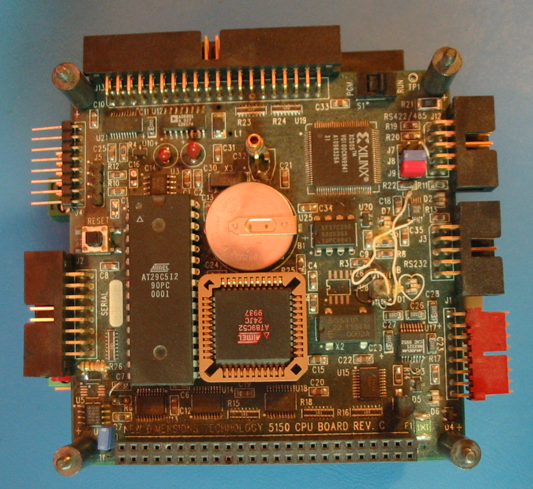
The CPU Board
Specification:
CPU: 8052 (clocked @ 22.118 MHz)
RAM: 32k bytes of battery backed (non-volatile)
ROM: 64k bytes (Flash)
BUS: 5150 bus 16 address lines, 8 data lines, 8-bit
digital I/O (port 1).
(see
schematic for pin-out details of J6)
Power:
+5.0V @ 250mA is required for operations. Supplied by J1 or thru the 5150 bus
connector J6 (see schematic for pin-out details).
Peripherals:
Data Acquisition:
8 channels of 8-bit DAC
8 channels or 4 differential channels of 12-bit ADC
(see schematic for pin-out details on connector J13)
RTC: Real Time Clock.
Ram memory location ( 0x0000 to 0x000D, see DS1384 data sheet for info.)
I/O:
LCD display connector (Standard 16 pin Optrex or other ASCII type LCD, Hitachi
based
HD447* controller, etc.) (connector J2)
4x4 Keypad connector (connector J4)
2-bit grey-code encoder connector (connector J5)
2 x 8-bit Digital I/O (connector J13)
(see schematic for pin-out details of J13)
Communications:
RS422/485 (J12 - Not working so don't bother.)
RS232 (J3 - Works. Use cable provided.)
Memory Map:
Rom: Address 0x0000 to 0xFFFF (64k)
RAM / RTC / Peripherals:
RTC: Address 0x0000 to 0x000D (14 bytes)
Ram: Address 0x000E to 0x7FFF (32k)
Available I/O address space: Address 0x8000 to 0xFFEF
Peripherals:
8-bit digital I/O Port 0 (R/W) Address: 0xFFF0
8-bit digital I/O Port 1 (R/W) Address: 0xFFF1
8-bit status register (R) Address: 0xFFF2
8-bit DAC data (W) Address: 0xFFF3
3-bit DAC address (W) Address: 0xFFF4
8-bit DAC command register (W) Address: 0xFFF5
8-bit ADC control byte / LS-byte of conversion register (R/W) Address: 0xFFF6
4-bit ADC command register / MS-nibble of conversion register (R/W) Address:
0xFFF7
8-bit Control Register (?) Address: 0xFFF8
8-bit NV Pot Register (W) Address: 0xFFF9
8-bit Encoder Register (R/W) Address: 0xFFFA
8-bit Keypad Register (R) Address: 0xFFFB
8-bit LCD Instruction Read (R) Address: 0xFFFC
8-bit LCD Instruction Write (W) Address: 0xFFFD
8-bit LCD Data Read (R) Address: 0xFFFE
8-bit LCD Data Write (W) Address: 0xFFFF
5150